The days of using a 20 watt soldering iron from Radio Shack are long gone when it comes to repairing lead free soldered circuits in Apple Computers, PCs, and other lead-free electronics equipment.
With multilayer boards, thick ground planes and power planes, and high temperature circuit board materials, along with countries having bans on the use of leaded solder in circuit boards; electronic components are now being attached using lead-free wave soldering or pick-and-place machines using conductive epoxy flux adhesives and then heat cured. All of this adds up to quite a bit of difficulty in reworking and repairing circuit boards today.
 While it is good to keep our environment clean, I think the wide spread use of lead-free solder in printed circuit board assembly processes is a case filled with a manufacturing life of unintended consequences. There are major challenges that have and continue to affect printed circuit board manufacturing around the world. First off, PCB materials must be able to withstand lead-free soldering temperatures of up to 260[degrees]C during the assembly operation. [1] This in itself, requires the use of more expensive, and much more difficult materials to work with at the PCB manufacturing stages. Not only is the multilayer construction much more difficult to deal with, but the drilling of the holes in thick multilayer circuit boards, with circuit board materials that are of a “harder” material nature, as compared to traditional FR-4 resin systems (not designed for lead-free), directly adds to the manufacturing costs involved.
I also find it interesting, that about the time where the world (pushed by the European Union) started converting over to using lead-free PCB manufacturing techniques, there seems to be a correlation between the electrolytic capacitor failures that started to occur a short time later in TVs, Set-Top Boxes, Computers, PCs from Dell, Apple, and other computer manufacturers, along with a host of other high powered electronic gadgets. I have no way of proving it, but I suspect that many of these components were hit with a large temperature blast through either high temperature wave soldering processes or oven based curing used in the finished component filled PCB assemblies.
“With a melting point of 217°C, SAC solder also is closest in melting point to the conventional lead–tin solder. This does mean, however, a yet-unquantified increase in energy use. Furthermore, the higher temperature may pose problems for the electronics industry. Higher temperatures mean more stress on components and the entire manufacturing process, notes Geibig. Higher temperatures also mean increases in the time it takes to make products, because more time is required to heat and cool the products during the course of their manufacture.” [2]
On July 1, 2006 the European Union Waste Electrical and Electronic Equipment Directive (WEEE) and Restriction of Hazardous Substances Directive (RoHS) came into effect, prohibiting the intentional addition of lead to most consumer electronics produced in the EU. California recently adopted a RoHS law and China has a version as well. [3] In order to meet the new directives established by the EU on removing the lead from electronics, has greatly affected the PCB assembly world at large. In effect, countries that did not have directives for the use of lead-free electronics assembly, were forced by default of having to build to meet the international requirements from the EU.
“This directive (EU Directive 2002/95/EC) places a restriction on the use of certain hazardous substances in electrical or electronic equipment sold or used in the European Union (EU) after July 1, 2006 with some exemptions.” [4]
‘Within the United States, California’s Electronic Waste Recycling Act imposes a fee on “covered electronic devices” currently being sold within the state. This fee is intended to cover the cost of properly disposing of the products when they become waste. Second, it requires “covered electronic devices” sold in California after January 1, 2007 to meet the same requirements as those found in European Union Restriction of Hazardous Substances (RoHS) legislation. Electronic devices containing toxic metals and not complying may not be manufactured, sold, or imported into California after January 1, 2007.’ [4] Other states have enacted similar laws.
So, what does that mean for circuit board and electronics repair folks today looking for ways to extend the service lives of their equipment? Well, there are some special soldering techniques that are involved to do the electronic repair jobs right.
What is required to repair lead-free circuit boards with large discrete components?
These lead-free soldering tips are specifically geared toward the large discrete components such as: electrolytic capacitors, transistors, diodes, bridge rectifiers, and coils (inductor chokes). Information on how to repair and replace surface mount devices with lead-free soldering techniques is waiting for a later date to be written.
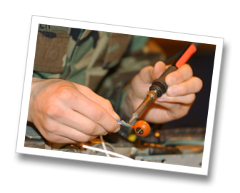
1. The minimum wattage for a soldering iron needs to be 60 watts. The 60 watts rating is only part of the specification to consider. Be aware that some soldering irons actually get hotter than others given the same wattage ratings. Additionally, you will need to consider using a proper soldering tip for the job at hand. If you are trying to solder on a thick multilayer PCB, then a wide tip is absolutely required to do the job right. There is also a difference in the coatings between the lead-free tips and the old standard Pb tips used for the standard 60/40 Tin Lead (60/40 Sn/Pb) Solder. 60/40 Sn/Pb melts at 370 °F or 188 °C while various lead-free solders used in PCB assembly have a melting point range of 415-441 °F or 213-227 °C . It is important to note that the increase in the melting temperature for lead-free solder, does not tell the whole story for proper solder joints involved with component replacements and PCB repairs.
You might be thinking, that the soldering iron I will be using gets up to 850 °F, I should be able to repair any lead-free soldered component on any PCB. That is wrong thinking here. I mentioned at the beginning about having a wide tip when soldering a thick multilayer. But, you need more than a wide tip. The soldering iron, at the tip, must be able to quickly recover on the heat cycle. It must also be able to supply the heat continually at a constant temperature, or near constant temperature to do the job right. This is where the wattage of the soldering iron is a factor for delivering the heat continually.
A thick multilayer PCB acts like a huge heatsink, sucking the heat away from the area that you want it, and dissipating it over the area where it is not required. If you use a small caliber soldering iron to try and remove components on this type of PCB, you will more than likely simply heat up the circuit board in a wide area, including the component itself before the solder will ever melt. In fact, it is quite likely that the lead-free solder will never melt, because the soldering iron can not quickly and effectively localize the heat in a high enough concentration to do any good. Actually you will probably do more harm than good.
I have heard from some folks, and talking from experience, that you will end up throwing a few choice words around that will not endear yourself to your spouse, if you try to use a low powered soldering iron. Even if you do manage to remove the component, the new component you install will have either the poorest of a solder joint, making you look like an amateur, or worse, an overly heated and damaged component that will result in early failure. Solder joints made with a low wattage soldering iron will likely result in cold solder joints, which will result in poor electrical connectivity and a non-working circuit board.
How about a portable butane powered soldering iron, won’t that work better? Been there and done that. Take it from experience, the answer to that question is no. I tried a wide tipped butane powered soldering iron and I was not able to even make a dent in the lead-free solder on a Apple iMac G5 motherboard.
What about a soldering gun? Once again, been there, done that. It doesn’t work with even the highest powered soldering gun. Soldering guns are not really designed for circuit board repairs. Take it from experience, put this idea out of your mind, it won’t work.
So Jim, what do you recommend in a soldering iron? Do you recommend a lead free soldering iron or a lead free soldering station? Let me first say here, that I have recommended some soldering irons and soldering stations to folks that have written to me and asked for my advice on various Apple repairs, and I would be more than happy to recommend something if you send me an email request. I will say this, that you can get a very good one at a very decent price. You don’t have to spend hundreds of dollars on a soldering station. However, don’t make the mistake and think you can get by with the old hobby soldering iron that you have in the desk drawer. Trying to use a substandard, low wattage soldering iron for lead-free motherboard repairs will give you headaches galore. Actually, I would like to hear more from readers of what you have used for lead free soldering.
2. What is the best way to remove the electronic component such as a electrolytic capacitor off a thick multilayer PCB once I have a good soldering iron or soldering station? I suggest you have the PCB standing up on edge, so that you can work from both sides of the circuit board. Check out the Chip Quik kit for removing the capacitors in difficult circuit boards. While heating up one leg of a radial electrolytic capacitor from the bottom, and at the same time slightly pushing the capacitor from the top, away from the leg being heated, at which time the solder starts to melt, the capacitor leg will start to move out of the hole. Do this for the other leg, alternating back and forth to each leg, and slowly work out the capacitor from the hole as the solder melts. After the capacitor is removed, a solder sucker can be used to remove a lot of the excess solder in and around the circuit pad. Using solder wick, (also referred to as desoldering wick or desoldering braid) on the thicker boards does not work well because of the extra heatsinking that occurs when the solder wick is applied. At this stage of the component replacement repair, invariably, not all the solder will come out of the holes with the use of a good quality solder sucker. This is where I suggest using my next soldering tip.
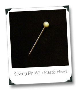
3. Try using a sewing pin, with a plastic head, (even a correct size safety pin works) and heat up the tip and the solder pad at the same time, once the caps are removed. This will push the solder out of the holes and solder will not stick to the steel sewing pins. Stop in at your local sewing machine center and you will find a large assortment of sewing pin sizes. Select a sewing pin size that matches up to the size of the leg of the capacitor. Once the pin is pushed through the hole, continue to apply heat to the pin and the pad, and move it in and out, making the hole the right size for your new components.
4. Is it best to use lead-free solder when installing the replacement capacitors? I have mixed thoughts on this. On the one hand, since the board is already using a lead-free solder, I would say stay with using lead-free solder. Yes, standard 60/40 lead solder is much easier to work with, due to its lower melting point, and some folks say it seems to work fine, but I have some reservations about using it. One negative item to be aware of here is that it is much more likely to end up getting cold solder joints when mixing solder types, and the other concern is, there may be a reduction in the soldering iron tip life if using the special plated tips designed for lead-free soldering, and using leaded solder.
I do have one major item that must be adhered to; only use a rosin core type of solder. Do not use acid flux. No acid flux. Acid core solder and acid flux will damage the circuit board and/or the components. With that being said, it is important that what ever solder is used, that the old solder and the new solder join (melt) together when installing the new components. Be careful with this that you don’t under heat or over heat your work. Just the right amount will do. It is hard to describe how much, and how long the heat should be applied to get a good solder joint. Take a close look at your solder joints. If they seem to be loose, then reapply the heat until the old and the new become one. As an additional note, and I have to say once again as a matter of importance, remember that the components themselves do not like it too hot for too long.
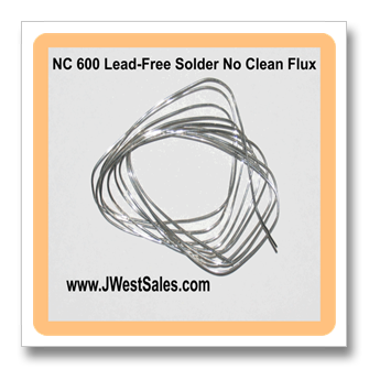
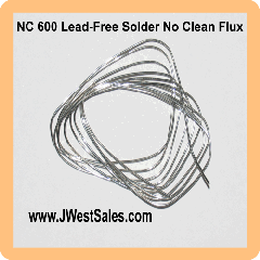 To properly solder motherboard capacitors on thick MOBs, you will need to operate the soldering iron or soldering station temperatures at or near maximum temperature settings. Heat up the pad on the bottom first and foremost by having most of the soldering tip on the pad; while at the same time having the tip touch the capacitor leg. I strongly suggest using lead free rosin core solder with a no clean residue; which you can purchase with your capacitors order at www.jwestsales.com. The no clean flux rosin core solder simply means that the center of the solder has a flux rosin core that is activated by heat, and the remaining residual flux does not need to be cleaned off the circuit board and will not harm the onboard circuitry. Remember also, that the MOB has residual lead free solder already present on the circuit pad and lining the circuit board hole walls, and must be melted (typically referred to as “wetting” action) with the new solder to form a good solder joint. If you use standard 60/40 lead solder for soldering, it is much more difficult to do the job just right, and is much more likely to produce cold solder joints because the different types of solders melt at substantially different temperatures and will not properly join together.
Be careful of other small components and surface mount devices (SMD) on the bottom and top of the boards. These devices are so small, that many times they can be damaged or unattached to the PCB simply by accidentally placing the soldering iron tip on the surface mounted component soldered leads, either moving it or bridging the leads with solder. So what I am saying is, try to use a steady hand.
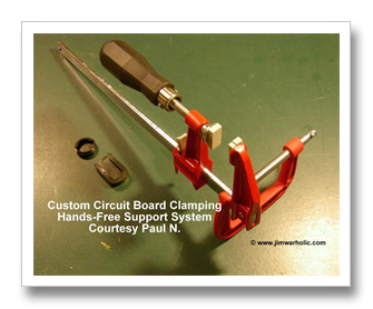
The picture above, of the custom circuit board clamping hands-free support system, is the brainchild of Paul N. — Grayslake, IL. Paul writes, “You can buy a 12″ x 2.5″ (depth) wood-working clamp from Home Depot for about $10 and a 3″ ‘C’ clamp for another $5. Then apply some adhesive-backed, dense foam rubber on each face of the wood-working clamp. Note that I removed the hard rubber covers that were on the clamp originally.” Paul calls the device the, “Kludged Circuit Board Clamp.” It is important to note that when clamping the circuit board with any clamping device, that you do not position the clamps on top of any components or the very small low profile SMDs on either side of the PCB.
There is another lead free soldering/unsoldering components helper that is simply amazing! Check out the video of the Chip Quik lead-free unsoldering kit and system of replacing components on circuit boards. I highly recommend this patented SMD and discrete components removal kit.
Read more about Apple iMac G5 Motherboard and Apple Power Supply Repairs.
Feel free to contact me at anytime.
Years of experience in the electronics industry. 🙂
Sources:
[1] The effects of lead-free on PCB fabrication: assemblers may bear most of the brunt of the…
[2] Getting the Lead Out of Electronics
[4] Why Should I Care About RoHS and Lead-Free Initiatives?

